Pascal GPU
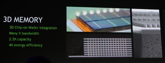
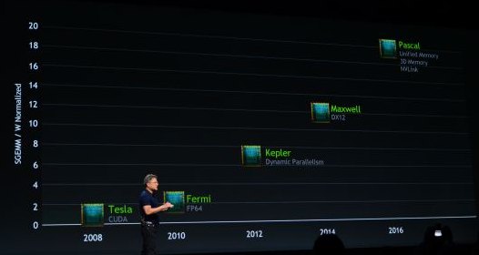
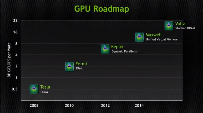
Pascal (from French mathematician Blaise Pascal) is Maxwell successor. In , we learnt that Volta was the post-Maxwell architecture, but it seems that Pascal is the new official name. One of the main feature of the Pascal architecture is the 3D memory or stacked DRAM that should provide terabyte bandwidth.
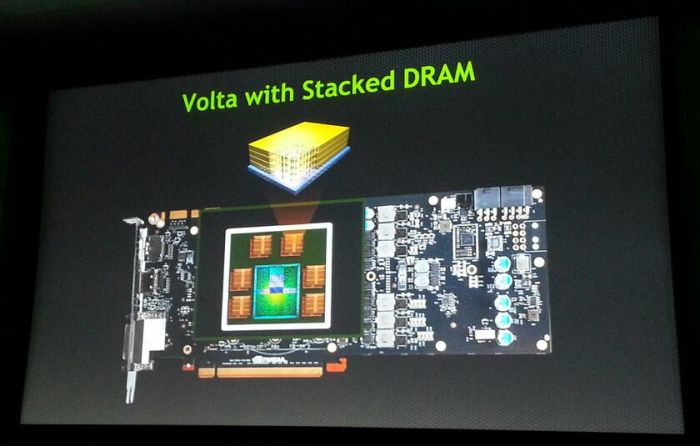
Update (2014.03.26): according to , Volta is the successor of Pascal:
Turns out Volta remains on the roadmap, but it comes after Pascal and will evidently include more extensive changes to Nvidia’s core GPU architecture.
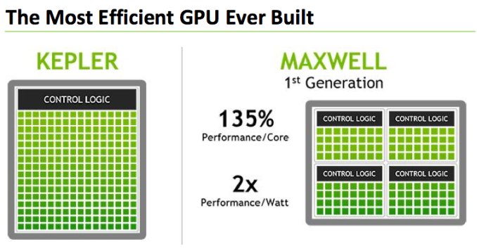
According to the guys at videocardz, NVIDIA Maxwell GM107 features 128 CUDA cores per SMX (streaming multiprocessor) against 192 for a Kepler-based GPU. The GeForce GTX 750 Ti has 5 SMX (640 cores) while the GTX 750 packs 512 cores in 4 SMX. The L2 cache has also received some changes: in Kepler the L2 cache has 256KB while on Maxwell, the cache has 2MB!
In the power consumption side, the GM107 has a TDP of 60W. And to finish, the GM107 will offer at least the same level (if not better) of performance than the GF100, the GPU behind the old good GTX 480.
Update (2013.03.20)
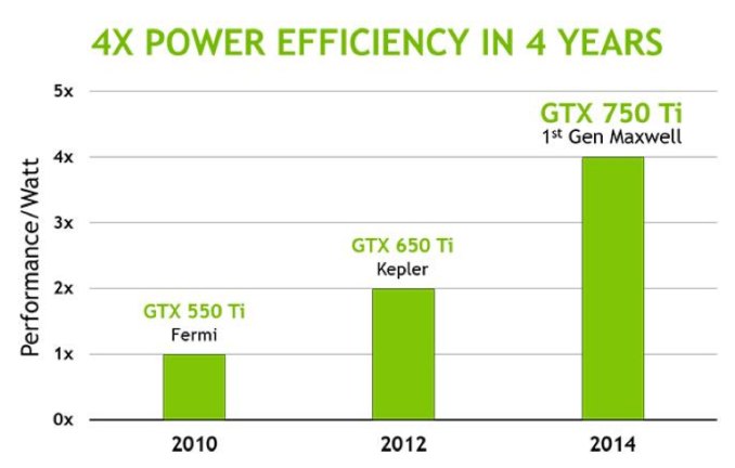
NVIDIA has just launched the first graphics cards based on Maxwell, NVIDIA’s new GPU architecture. The and are both powered by a GM107, a cut down version of an upcoming flagship (GM110 ?) GPU. The Maxwell architecture is focused on power efficiency:
Kepler SMXs (streaming multiprocessors) are now replaced by Maxwell SMMs. A SMM packs 128 CUDA cores(SMX = 192 cores). The L2 cache size has been increased from 256KB in Kepler to 2048KB in Maxwell.
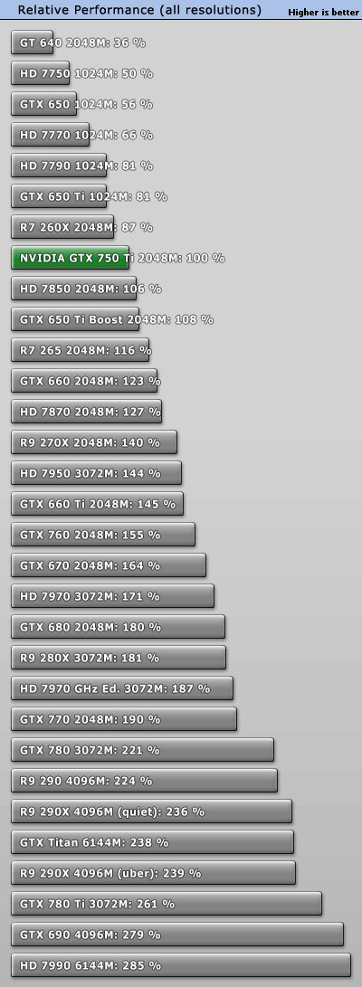
The new GTX 750 and GTX 750 Ti targets the old GeForce GTX 650 Ti and the recently launched .
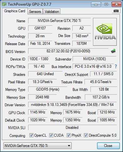
GeForce GTX 750 Ti specifications
- GPU: GM107 @ 1020MHz (base) / 1085MHz (boost), 28nm
- Cores: 640 (5 SMMs)
- Texture units: 40
- ROPs: 16
- Memory: 2048MB @ 5.4GHz GDDR5, 128-bit
- TDP: 60W
- Price: USD $149
GeForce GTX 750 specifications
- GPU: GM107 @ 1020MHz (base) / 1085MHz (boost), 28nm
- Cores: 512 (4 SMMs)
- Texture units: 32
- ROPs: 16
- Memory: 1024MB @ 5.0GHz GDDR5, 128-bit
- TDP: 55W
- Price: USD $119